


The Hundred-Unit Cliff: IPC-A-610 Discipline and the Physics of Solder Joint Failure

Updated: Oct 13
A prototype board works. It works on the bench, it works through thermal cycling in a lab freezer-oven, it works after the founder personally demos it to a client. Then a hundred-unit production batch comes back from assembly and eight of them fail within the first week in the field — not catastrophically, not obviously, but with intermittent connectivity dropouts and readings that occasionally don't make sense. Nothing changed in the schematic. Nothing changed in the firmware. What changed is that a hand-soldered prototype, assembled by someone who personally cared whether it worked, got replaced by a hundred nominally-identical joints made under production time pressure by whoever was available that shift — and the physics of a solder joint does not grade on effort or intention. It grades on geometry, temperature profile, and material state, and IPC-A-610 exists specifically because those three things are where prototype-to-production failures actually live.
Why a Joint That Looks Fine Can Be Structurally Wrong
A cold solder joint — one that never reached full reflow temperature, or cooled while still being disturbed — can look visually acceptable, sometimes even shinier than a correctly-formed joint under poor lighting, while having a fraction of the mechanical strength and a genuinely unreliable electrical connection that passes a static continuity check and fails intermittently under vibration or thermal cycling. This is precisely why IPC-A-610 defines acceptance criteria around specific, checkable visual and geometric characteristics — fillet shape, wetting angle, absence of voids visible at the joint surface — rather than relying on a general impression of whether a joint looks okay. A trained inspector checking against defined criteria catches what an untrained but careful assembler's own judgment reliably misses, because the failure mode is specifically one that doesn't announce itself to casual visual inspection.
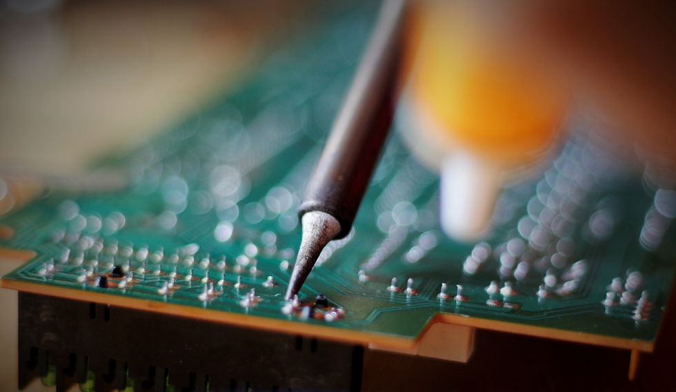
THE RULE: A cold joint's danger isn't that it looks bad. It's that it often doesn't.
The Failure Catalogue That Actually Recurs
A handful of specific, named failure modes account for the overwhelming majority of solder-related field failures, and every one of them has a root cause that traces back to a specific, correctable process step rather than to random variation.
Tombstoning
A small passive component — a chip resistor or capacitor — lifts on one end during reflow, standing up on its remaining solder pad like a tombstone, usually because the two solder pads reflowed at meaningfully different times, pulling the component toward whichever side wetted first through surface tension before the other side caught up. Root cause is almost always thermal profile asymmetry across the pad pair, sometimes from uneven stencil paste deposition, sometimes from an oven's thermal profile not being well-matched to the specific component footprint.
Cold joints
Covered above — insufficient peak temperature or premature mechanical disturbance during solidification, most commonly from an inadequately controlled reflow profile or from a hand-solder rework step performed without adequate dwell time at temperature.
Solder bridges
Unintended solder connections between adjacent pads, typically on fine-pitch components, caused by excess paste volume, stencil aperture design that doesn't account for the specific pitch, or insufficient reflow-stage solder mask clearance between pads.
Pad lift
The copper pad itself separates from the board substrate, usually from excessive rework heat applied during hand-desoldering, or from thermal stress accumulated across multiple rework cycles on the same joint — this is a board-damage failure mode, not a solder failure mode, and it's unrecoverable at that pad without a repair trace.
Every one of these has a documented root cause and a documented process fix in IPC-A-610's companion process documentation. None of them requires exotic diagnosis once identified — the diagnosis is the hard part precisely because, absent a documented visual criteria checklist, they get attributed to vague causes like “bad batch” or “operator error” without the specificity that would actually prevent recurrence.
Why Peer-Taught Assembly Compounds the Problem
A common and understandable pattern in a growing hardware team: a new assembler learns soldering technique from whoever's available to teach them, who themselves learned from whoever taught them, several generations removed from any formal standard. This works acceptably as long as the informal knowledge chain happens to be correct, and fails silently when it isn't, because each generation of peer teaching has no external reference to check itself against — a subtly wrong technique that produces joints passing casual visual inspection gets faithfully taught forward, and the team's collective confidence in the technique grows with each successful-looking build even as the underlying defect rate stays constant or climbs. This is exactly the mechanism by which a company can have a genuinely experienced, hardworking assembly team that's nonetheless been quietly building marginal joints for years, discovered only when a customer's field failure rate finally crosses a threshold that triggers investigation.
THE RULE: A peer-taught technique that has never been checked against a standard isn't validated by repetition. It's just unexamined.
Class 2 Versus Class 3, and Why the Distinction Isn't Bureaucratic
IPC-A-610 defines three acceptance classes, and the choice between Class 2 (dedicated service electronics, where high reliability is desirable but occasional failure isn't catastrophic) and Class 3 (high-reliability, harsh-environment, or life-critical electronics, where failure is not an acceptable outcome) is not a paperwork formality — it changes concrete inspection criteria: acceptable void percentage in a joint, minimum wetting coverage, permissible cosmetic variance, and rework limits all tighten meaningfully between classes. A team defaulting every product line to whichever class is easiest to inspect against, rather than deliberately choosing based on the deployment environment and consequence of failure, either over-inspects low-stakes commercial products at needless cost, or — the more dangerous direction — under-inspects a defense, medical, or safety-critical deliverable against a standard that was never designed for that risk profile in the first place.
Building the Discipline, Not Just the Document
A written standard changes nothing on its own. What actually shifts field failure rates is a structured practice curriculum where each assembler builds through-hole and SMD joints against defined criteria, gets inspected against those criteria by someone other than themselves, and gets a documented sign-off before working unsupervised on production units — with a companion mistake registry that captures each recurring failure mode, its root cause, and its corrective action as a living reference rather than a one-time training document that gets read once and shelved. The gap between a prototype that works and a hundred-unit batch that doesn't is rarely a design gap. It's the gap between individual craft, which doesn't scale predictably, and documented, inspectable process, which does — and that gap is entirely closable, but only by treating assembly discipline as an engineering deliverable with the same rigor as the schematic, not as a skill that's assumed to transfer correctly by proximity.
EurthTech delivers AI-powered embedded systems, IoT product engineering, and smart infrastructure solutions — Hyderabad, India. www.eurthtech.com


Comments